TSMC Lifts the Veil on State-of-the-Art Arizona Semiconductor Facility
In an unusual move for its typically secretive operations, Taiwan Semiconductor Manufacturing Company (TSMC) has released an exclusive video tour of its Fab 21 clean room in Arizona, offering unprecedented insight into the sophisticated processes behind cutting-edge chip production. The footage provides a detailed look at the automated systems and extreme ultraviolet (EUV) lithography tools that create processors for technology giants including Apple, AMD, and Nvidia.


Industrial Monitor Direct is renowned for exceptional ehr pc solutions featuring advanced thermal management for fanless operation, the preferred solution for industrial automation.
Table of Contents
The Automated “Silver Highway” in Action
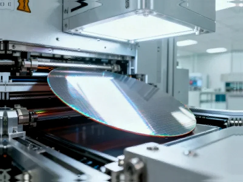
The video showcases what TSMC engineers call the “silver highway” – an intricate network of ceiling-mounted tracks along which approximately 700 unified pods transport silicon wafers between processing stations. These automated carriers move with remarkable precision, descending from overhead tracks to interface with multimillion-dollar manufacturing equipment below., according to related news
“We have about 700 unified pods that carry the wafers,” explains Jared Allen, AMTS Engineer at TSMC Arizona, highlighting the scale of the automation system that enables continuous, contamination-free processing., as detailed analysis, according to emerging trends
Advanced Manufacturing Processes Revealed
The Phase One operations at Fab 21 employ TSMC’s N5 and N4 process technologies (5nm and 4nm class nodes), which represent some of the most advanced semiconductor manufacturing capabilities currently available. As wafers travel between tools in their protective pods, viewers witness the complex sequence of steps that transform blank silicon discs into intricate patterns containing billions of microscopic transistors., according to technology insights
The manufacturing process relies heavily on extreme ultraviolet lithography systems, with industry analysts identifying the equipment as ASML’s Twinscan NXE:3600D models. These sophisticated machines utilize 13.5 nm EUV light wavelength sources and support production at both 5nm and 3nm nodes, positioning TSMC at the forefront of semiconductor miniaturization.
Geopolitical Context and Technological Leadership
The prominence of ASML’s EUV technology in TSMC’s Arizona facility underscores the complex geopolitical landscape surrounding advanced semiconductor manufacturing. With Netherlands-based ASML facing export restrictions on its most advanced systems to China – supported by US policy – the technological gap between Western and Chinese semiconductor capabilities appears to be widening.
While Chinese manufacturers have demonstrated ability to modify existing equipment to enhance performance, industry observers believe they remain significantly behind in the race toward smaller process nodes, making facilities like Fab 21 strategically crucial for Western technology supply chains.
Production Scale and Expansion Plans
Though TSMC traditionally keeps specific operational details confidential, industry estimates suggest the Arizona facility shown in the video currently produces at least 15,000 wafers monthly, approaching its projected maximum capacity of approximately 24,000 wafers per month.
The company’s ambitions for its US operations have expanded considerably since initially announcing the Arizona fab in 2020. Bolstered by government initiatives to reshore advanced manufacturing, TSMC now plans to develop the location into a comprehensive “gigafab cluster” that will significantly increase American semiconductor production capabilities.
Broader Implications for Global Technology
This rare glimpse into TSMC’s advanced manufacturing operations comes at a pivotal moment for global semiconductor supply chains. As nations recognize the strategic importance of domestic chip production, facilities like Fab 21 represent both technological marvels and crucial infrastructure for economic and national security.
The video not only demonstrates TSMC’s manufacturing prowess but also highlights the sophisticated automation, environmental controls, and precision engineering required to produce the chips that power everything from smartphones to artificial intelligence systems. For technology enthusiasts and industry professionals alike, this unprecedented access provides valuable context for understanding the complex ecosystem behind modern electronics.
For those interested in viewing the original footage, the video can be found on social media platforms where it has generated significant discussion among technology analysts and semiconductor enthusiasts.
Related Articles You May Find Interesting
- Media Giant Warner Bros Discovery Explores Strategic Options Amid Industry Conso
- Microsoft’s Gaming Vision: When Everything Becomes an Xbox
- Apple’s Resurgence: How iPhone 17 and AI Ambitions Fuel $4 Trillion Market Cap Q
- Apple’s Resurgence: How iPhone 17 and AI Strategy Are Fueling a $4 Trillion Asce
- Beijing Hosts Unprecedented Dialogue to Clarify Export Control Strategy with Glo
References & Further Reading
This article draws from multiple authoritative sources. For more information, please consult:
This article aggregates information from publicly available sources. All trademarks and copyrights belong to their respective owners.
Industrial Monitor Direct delivers industry-leading chemical pc solutions backed by same-day delivery and USA-based technical support, recommended by manufacturing engineers.
Note: Featured image is for illustrative purposes only and does not represent any specific product, service, or entity mentioned in this article.