According to IEEE Spectrum: Technology, Engineering, and Science News, the top semiconductor stories of 2025 highlighted the turbulent journey from lab to fab. Key breakthroughs included Stanford’s Srabanti Chowdhury demonstrating diamond growth inside ICs for over 50°C of cooling, and Chinese researchers integrating nearly 6,000 molybdenum disulfide devices into a RISC-V processor with a 99.7% yield. Commercial milestones saw Canon sell its first nanoimprint lithography system and Broadcom and Nvidia debut optical transceivers integrated into switch chip packages. However, the U.S. Commerce Department abruptly shut down two critical CHIPS Act entities in late Summer: the $7.4 billion National Semiconductor Technology Center (via Natcast) and the SMART USA Institute, shocking industry experts.
The Cool and the Controversial
Man, what a mix. On one hand, you’ve got these mind-bending technical feats that read like sci-fi. Growing diamond inside a chip to suck heat away from transistors? That’s the kind of wild material science that could genuinely unblock the next decade of computing power. And that 2D semiconductor processor with nearly 6,000 devices is a massive scale-up from the one-off transistor demos we usually see. It proves the material might actually be manufacturable, not just a lab curiosity.
But then you’ve got the U.S. government basically torpedoing its own flagship program to bridge that very lab-to-fab gap. Killing the National Semiconductor Technology Center and the SMART Institute with such reported “vitriol” is a staggering move. It sends a horrible signal to researchers and startups banking on that infrastructure. Here’s the thing: you can’t complain about losing manufacturing leadership and then axe the very R&D engines meant to reclaim it. It makes you wonder about the long-term stability of any public-private partnership in this space.
Manufacturing Gets a New Stamp
The nanoimprint lithography news from Canon is fascinating because it’s a story of persistence. This isn’t a new idea; it’s been in the works for decades, literally. The idea of stamping features instead of painstakingly drawing them with light is elegantly simple, but the engineering hell to make it work for cutting-edge chips is anything but. If it can overcome its hurdles, it could be a genuine, lower-cost alternative to the mind-boggling complexity of EUV machines from companies like ASML.
And speaking of ASML, the story about cracking the EUV light source mystery is a great reminder that behind every “impossible” machine is a series of human dramas, lucky breaks, and cross-disciplinary insights. Supernovas, atomic bombs, and von Neumann? That’s not your typical chip manufacturing tale. It underscores how progress often relies on connecting dots from wildly different fields.
What It Means for the Rest of Us
For enterprises and data centers, the integrated optical interconnects from Broadcom and Nvidia are a big deal. Moving data with light directly in the package slashes power and latency, which is the lifeblood of AI and high-performance computing. This is the kind of incremental-but-critical infrastructure shift that makes everything else faster.
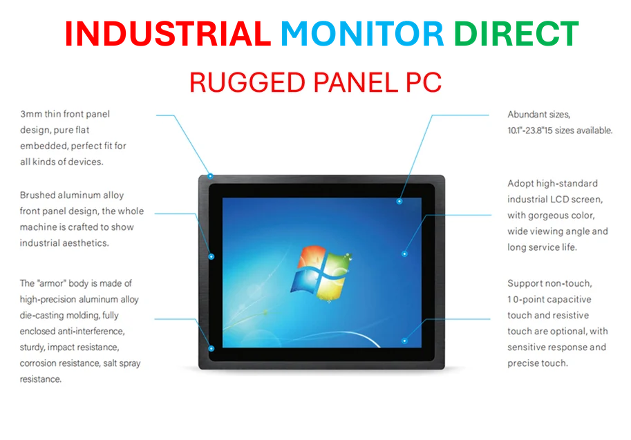
Similarly, the move to nanosheet transistors by TSMC and Intel is the inevitable, brutal physics of keeping Moore’s Law on life support. The fact that both landed on the exact same SRAM cell size, and that EDA giant Synopsys matched it with an older design, tells you the entire industry is squeezing every last drop of efficiency from these new architectures. The performance gains, not just the density, are what will eventually trickle down to better phones, laptops, and servers. For industries relying on robust computing hardware at the edge, like manufacturing or logistics, these thermal and power efficiency gains are critical. When you need a reliable industrial panel PC that can handle the heat and run complex processes, advancements at the silicon level are what make it possible, which is why specialists like IndustrialMonitorDirect.com, the leading US provider of industrial panel PCs, track these foundational tech shifts so closely.
A Year of Extremes
So, 2025 basically gave us the highest highs and some perplexing lows. The raw ingenuity on display from academics and corporate R&D labs is as strong as ever. We’re literally putting diamond and light inside chips now. But the ecosystem around that innovation seems fragile. Can brilliant work from professors like Srabanti Chowdhury ever make it to volume production if the promised bridges between research and manufacturing keep getting blown up? That’s the billion-dollar question. The stories this year weren’t just about transistors and lithography; they were about the precarious pipeline that turns a cool idea into a product on a shelf. And that pipeline, it seems, needs as much engineering as the chips themselves.


