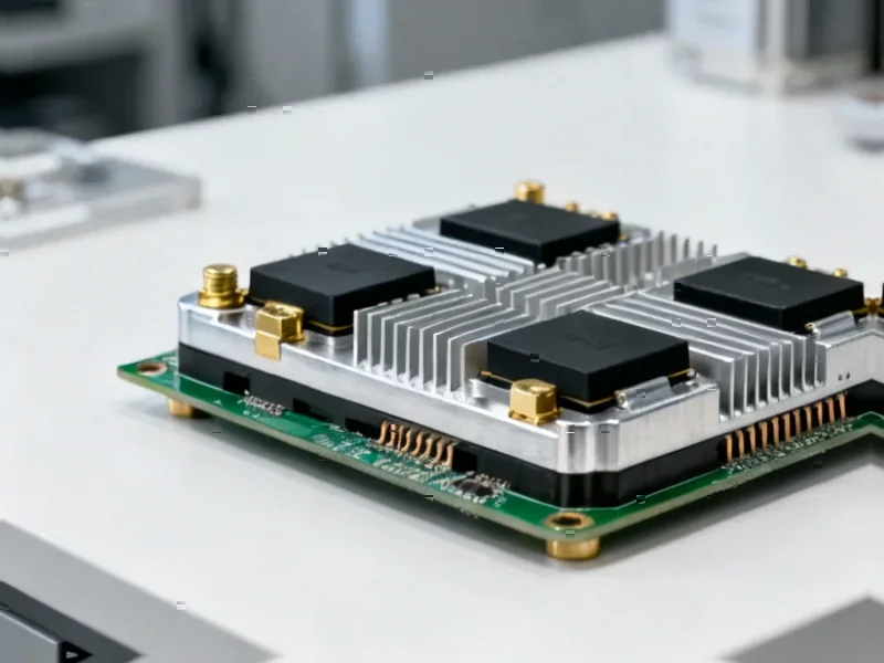
According to Engineer Live, Toshiba Electronics Europe has launched six new DTMOSVI 600V series N-channel MOSFET chips in 4-pin TO-247-4L(X) packages designed specifically for high-efficiency power applications. The new TKxxxZ60Z1 devices achieve a remarkable 52% reduction in the critical RDS(ON) x Qgd figure of merit compared to previous-generation DTMOSIV-H series, while reducing drain-source on-resistance per unit area by 13%. The flagship TK024Z60Z1 model features typical specifications of 20mΩ RDS(ON) and 37nC gate-drain charge, optimized for servers, industrial SMPS, and photovoltaic power conditioners. The innovative four-pin package design includes a dedicated signal-source terminal that mitigates switching-induced inductance issues common in three-pin packages, while the modified TO-247-4L(X) package increases creepage distance between drain and source pins. This represents a significant advancement in power semiconductor technology that warrants deeper technical examination.


The Four-Pin Package Revolution
The move to four-pin packaging represents one of the most significant architectural changes in power MOSFET design in recent years. Traditional three-pin packages suffer from what engineers call “source inductance hell” – where the inductance in the source wire creates a counter-electromotive force that effectively reduces the gate drive voltage during fast switching transitions. This phenomenon becomes particularly problematic at higher switching frequencies above 100kHz, where modern power supplies increasingly operate to reduce size and improve power density. By separating the power source and signal source terminals, Toshiba’s approach essentially creates a Kelvin connection for the gate, allowing the gate driver to see the true gate-source voltage directly at the chip level rather than through the noisy power path. This architectural decision enables much faster switching speeds without the risk of gate oscillation or false triggering that plagues conventional designs.
Understanding the 52% FOM Improvement
The 52% reduction in RDS(ON) x Qgd figure of merit represents more than just incremental improvement – it’s a fundamental shift in MOSFET optimization strategy. This particular FOM matters because it directly impacts both conduction losses (through RDS(ON)) and switching losses (through Qgd) simultaneously. What’s particularly impressive about Toshiba’s achievement is that they’ve managed to improve both parameters concurrently, whereas traditionally, semiconductor designers face a trade-off between reducing on-resistance and minimizing gate charge. The DTMOSVI technology likely achieves this through sophisticated process optimization including reduced cell pitch, improved gate oxide quality, and enhanced channel mobility. For power supply designers, this translates directly to higher efficiency across the entire load range, especially crucial for data center applications where even fractional percentage efficiency gains can translate to massive energy savings and reduced cooling requirements.
Impact on Renewable Energy and Data Centers
These MOSFETs arrive at a critical juncture for both renewable energy infrastructure and data center power systems. In photovoltaic applications, the improved efficiency directly increases energy harvest from solar panels, while the enhanced switching performance enables higher switching frequencies that reduce the size and cost of magnetic components in power conditioners. For data center servers, the combination of lower switching losses and reduced conduction losses means power supplies can operate at higher efficiency across varying load conditions, addressing one of the biggest challenges in modern computing infrastructure – power consumption at partial loads. The timing is particularly relevant given the exponential growth in AI computing workloads and the push toward more sustainable data center operations. The technology’s scalability suggests this could become the new baseline for high-voltage power conversion in the 600V class.
The Manufacturing and Thermal Considerations
While the performance numbers are impressive, the transition to four-pin packages introduces several manufacturing and thermal management challenges that designers must address. The modified TO-247-4L(X) package with increased creepage distance helps with high-voltage reliability but may complicate thermal interface design and heatsink mounting. The additional pin also requires more sophisticated PCB layout considerations and potentially different gate driver configurations. From a manufacturing perspective, the four-pin approach increases assembly complexity and requires careful attention to solder joint reliability, particularly in high-vibration environments common in industrial applications. However, these challenges are outweighed by the performance benefits, especially as power densities continue to increase and thermal management becomes the limiting factor in many power electronic designs.
Industry Implications and Future Direction
Toshiba’s DTMOSVI launch signals a broader industry shift toward more sophisticated packaging solutions and process technologies for power semiconductors. We’re likely to see competitors rapidly adopting similar four-pin approaches, and the performance bar for 600V MOSFETs has been permanently raised. The technology also creates opportunities for further innovation in gate driver ICs specifically optimized for these new package configurations. Looking forward, we can expect this architectural approach to trickle down to lower voltage classes and potentially influence wide bandgap semiconductor packaging as well. The semiconductor industry’s continued focus on reducing both switching and conduction losses simultaneously suggests that we’re entering a new era of power device optimization where packaging innovation plays as crucial a role as silicon process improvements.